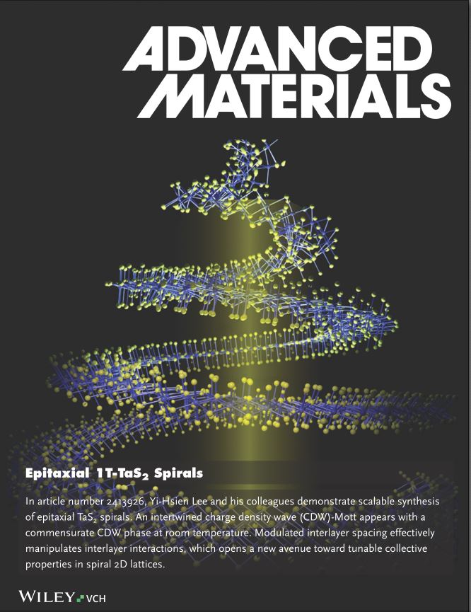
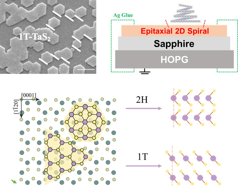
Tunable Electron Correlation in Epitaxial 1T-TaS2 Spirals
Chung-Jen Chen, C.A. Chen, Y.X. Zheng, C.T. Chung, Y.T. Lin, Y.C. Chiang, Ting-Kuo Lee, Yi-Hsien Lee*
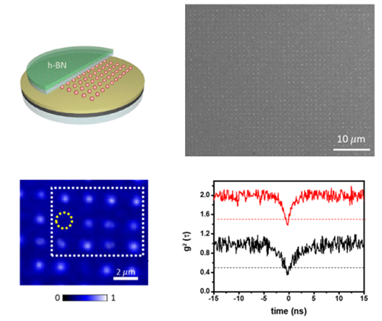
Tunable Single-Photon Emission with Wafer-Scale Plasmonic Array
Chun-An Chen, P.H. Chen, Y.X. Zheng, C.H. Chen, M.K. Hsu, K.C. Hsu, Y.Y. Lai, C.S, Chuu, Hui Deng, Yi-Hsien Lee*
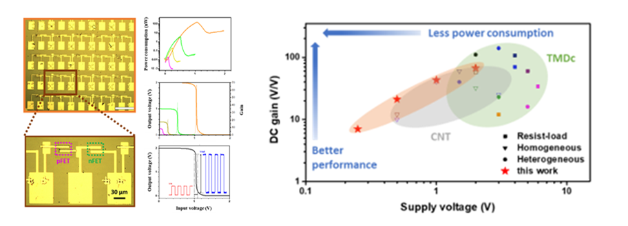
Integrated Low Dimensional Semiconductors for Scalable Low-power CMOS Logic
M.H. Chuang, K.C. Chiu, Y.T. Lin, P.H. Chen, A. Pezeshki, C.J. Chen, P.Y. Chen,
L.J. Chen, S.J. Han, Yi-Hsien Lee*
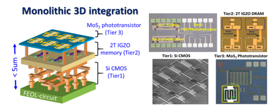
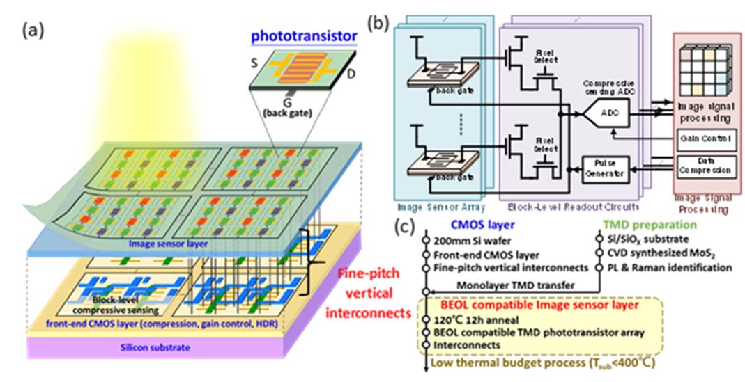
3D Monolithically Integrated Device of Si CMOS Logic, IGZO DRAM-like, and 2D MoS2 Phototransistor for Smart Image Sensing
F.M. Lee*, P.H. Tseng, Y.Y. Lin, Y.H. Lin, W.L. Weng, N.C. Lin, P.J. Sung, C.C. Yang*, W.F. Wu, C.H. Shen, P.H. Chen, Yi-Hsien Lee*, M.H. Lee, K.C. Wang, and C.Y. Lu
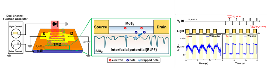
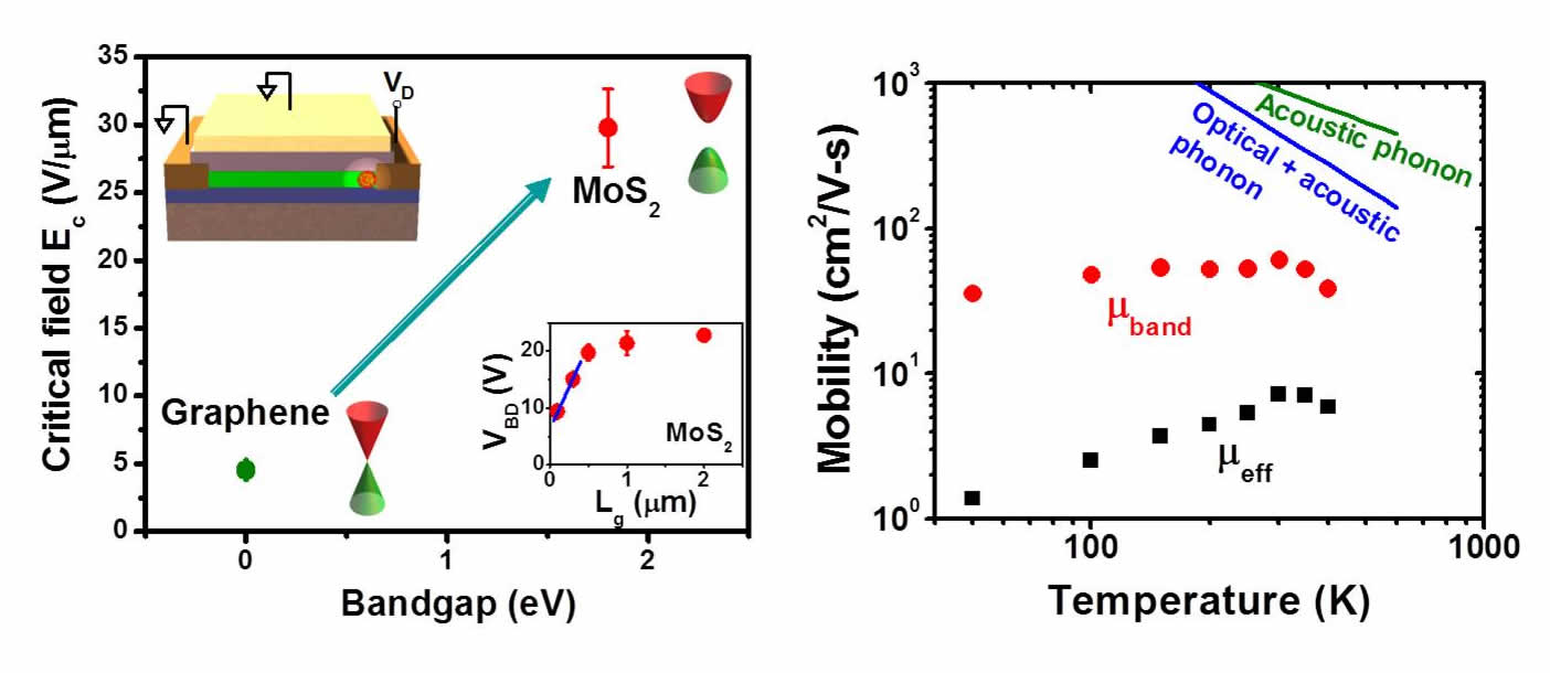
Passivated Interfacial Traps of Monolayer MoS2 with Bipolar Electrical Pulse
Po‐Han Chen, C.A. Chen, Y.T. Lin, P.Y. Hsieh, M.H. Chuang, X. Liu, T.Y. Hsieh, C.H. Shen, J.M. Shieh, M.C. Wu, Y.F. Chen, C.C. Yang*, Yi-Hsien Lee*
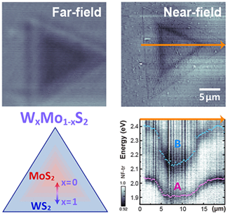
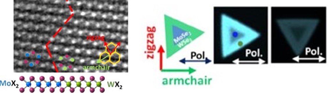
Visualization of Band Shifting and Interlayer Coupling in WxMo1–xS2 Alloys Using Near-Field Broadband Absorption Microscopy
Po-Wen Tang, Shiue-Yuan Shiau, He-Chun Chou, Xin-Quan Zhang, Jia-Ru Yu, Chun-Te Sung, Yi-Hsien Lee*, Chi Chen*
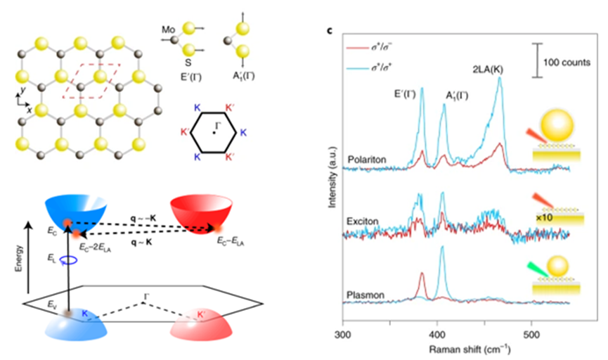
Nonlinear valley phonon scattering under the strong coupling regime
Xiaoze Liu, J. Yi, S. Yang, Erh-Chen Lin, Y.J. Zhang, P. Zhang, J.F. Li, Y. Wang, Yi-Hsien Lee, Zhong-Qun Tian, Xiang Zhang
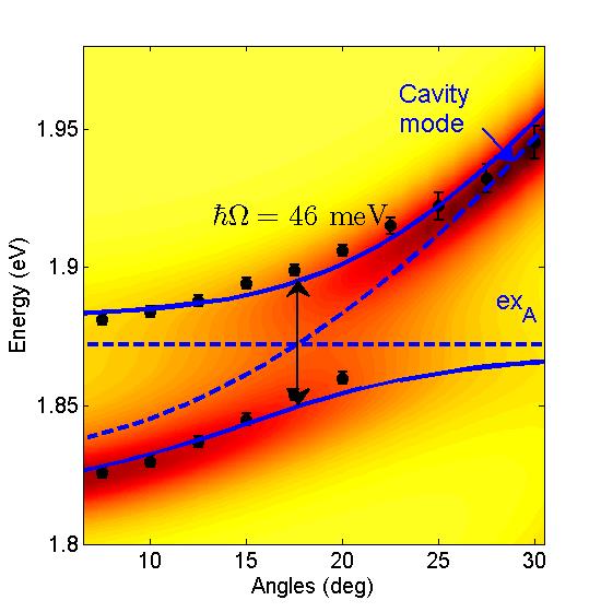
Tuning of Two-Dimensional Plasmon–Exciton Coupling in Full Parameter Space
Y. Sang, CY Wang, S. Raja, CW Cheng, CT Huang, CA Chen, XQ Zhang, H. Ahn, Hyeyoung; CK Shih, Yi-Hsien Lee, J. Shi, Shangjr Gwo
Ultrahigh responsivity and tunable photogain BEOL compatible MoS2 phototransistor array for monolithic 3D image sensor with block-level sensing circuits
Chih-Chao Yang*, P.Y. Hsieh, Po‐Han Chen, TY Hsieh, P.T. Huang, Yu-Ting Lin, C.H. Shen, J.M. Shien, D.C. Chang, W.K. Yeh, M.C. Wu, Yi-Hsien Lee*
Epitaxial Aluminum Surface-Enhanced Raman Spectroscopy Substrates for Large-Scale 2D Material Characterization
Soniya S Raja, C.W. Cheng, Y. Sang, C.A. Chen, X.Q. Zhang, A. Dubey, T.J. Yen, Y.M. Chang, Yi-Hsien Lee, Shangjr Gwo
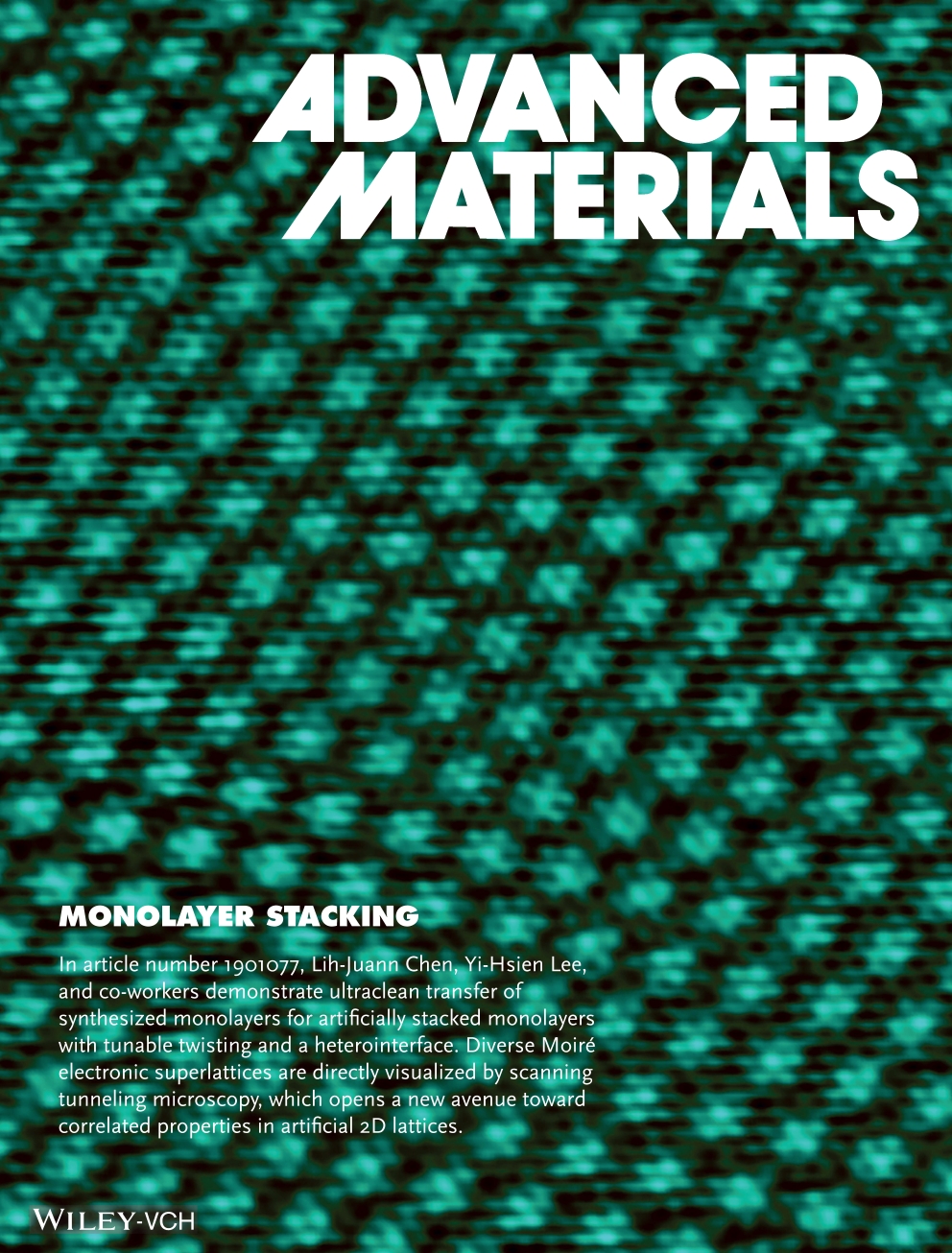
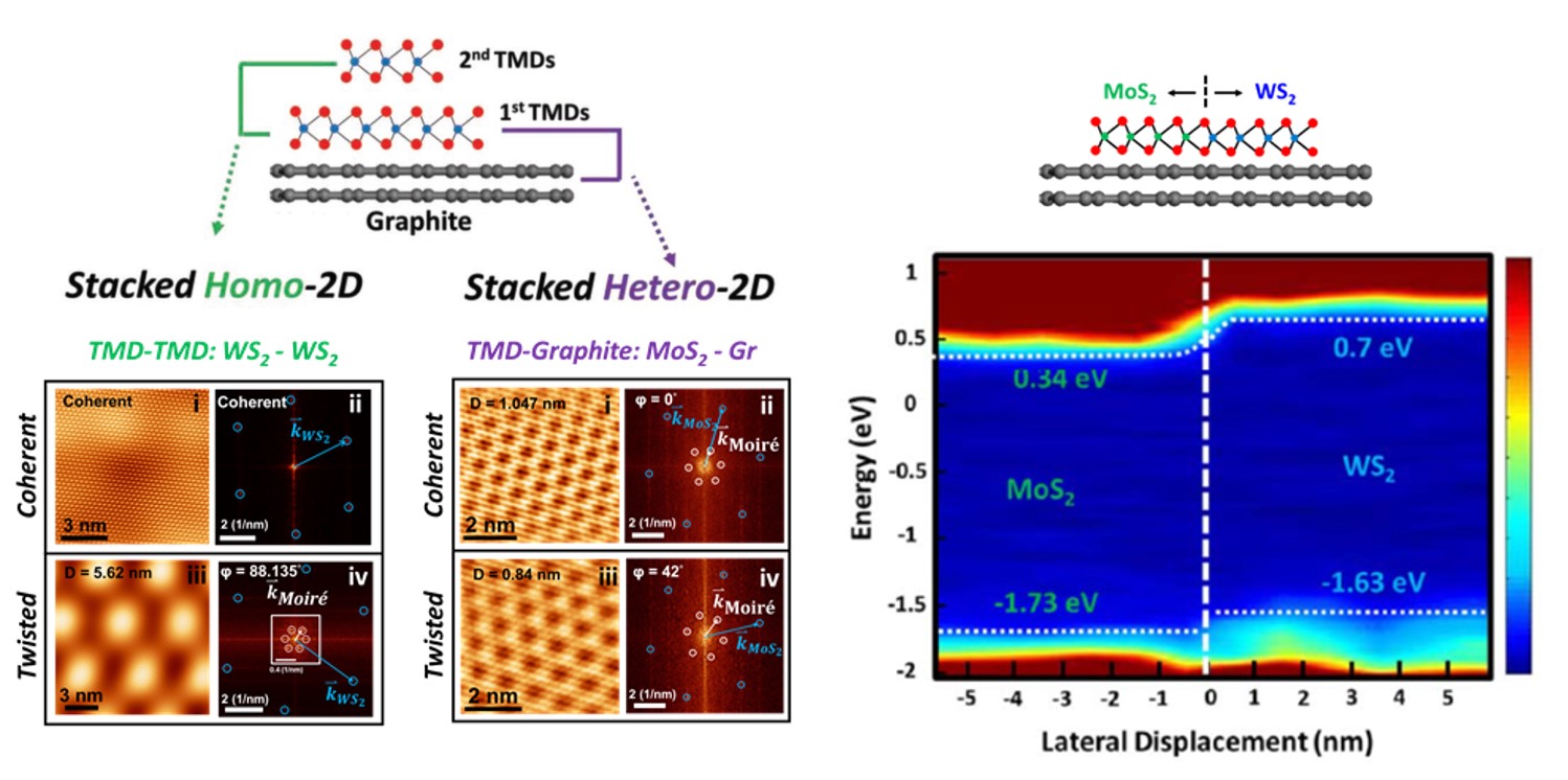
Tunable Moiré Superlattice of Artificially Twisted Monolayers
Po-Yen Chen, X. Zhang, Y. Lai, E. Lin, C. Chen, S. Guan, J. Chen, Z. Yang, Y. Tseng, S. Gwo, C.S. Chang, Lih-Juann Chen*, Yi-Hsien Lee*
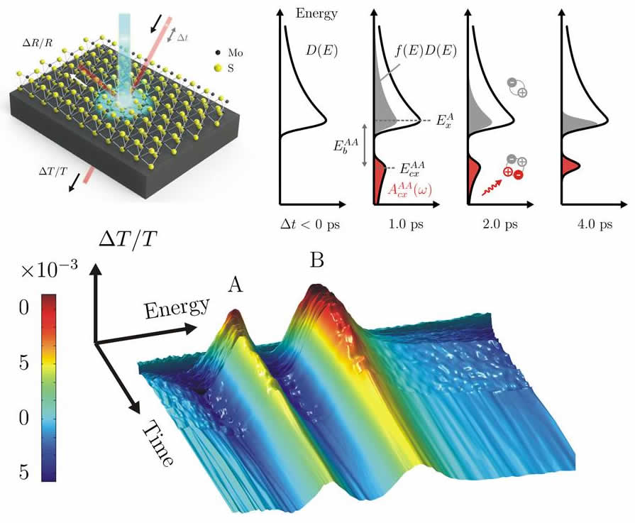
Exchange-driven mixing of A and B excitons in monolayer transition metal dichalcogenides
Liang Guo, M. Wu, T. Cao, D. Monahan, Yi-Hsien Lee, Steven G. Louie, Graham R. Fleming
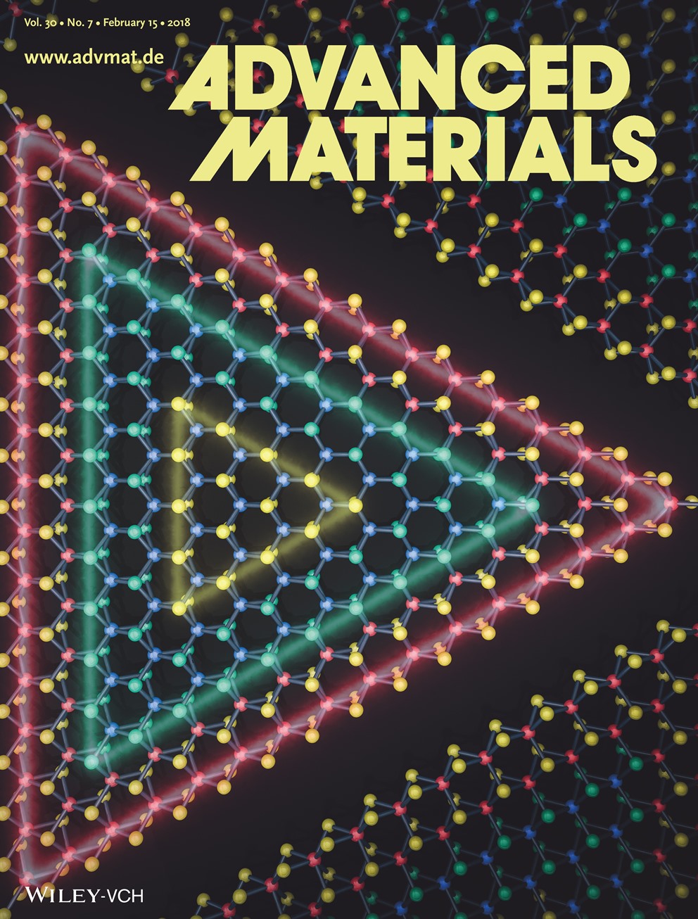
Synthesis of In-plane Artificial Lattices of Monolayer Multi-junctions
Kuan-Chang Chiu, K.H. Huang, C.A. Chen, Y.Y. Lai, X.Q. Zhang, E.C. Lin, M.H. Chuang, J.M. Wu, Yi-Hsien Lee*
A Gate-free Monolayer WSe2 p-n Diode
Jhih-Wei Chen et.al.
Observation of Exciton–Exciton Interaction Mediated Valley Depolarization in Monolayer MoSe2
Fahad Mahmood, Z. Alpichshev, Yi-Hsien Lee, J. Kong, Nuh Gedik*
Autocatalytic Surface Reduction and Its Role in Controlling Seed-Mediated Growth of Colloidal Metal Nanocrystals
Tung-Han Yang, S. Zhou, Kyle D. Gilroy, Legna Figueroa-Cosme, Yi-Hsien Lee, J.M. Wu, Younan Xia*
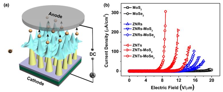
Electron Field Emission of Geometrically-Modulated Monolayer Semiconductors
Tung-Han Yang, K. Chiu, Y. Harn, H. Chen, R. Cai, J. Shyue, S. Lo, J. M. Wu, Yi-Hsien Lee*
Cascaded Exciton Energy Transfer in a Monolayer Semiconductor Lateral Heterostructure Assisted by Surface Plasmon Polariton
Jinwei Shi, M. Lin, Yi-Tong Chen, N.M. Estakhri, Xin-Quan Zhang, Y. Wang, H. Chen, Chun-An Chen, Chih-Kang Shih, Andrea Alù , Xiaoqin Li*, Yi-Hsien Lee*, Shangjr Gwo*
Strong and broadly tunable plasmon resonances in thick films of aligned carbon nanotubes
Kuan-Chang Chiu, Abram L. Falk, Po-Hsun Ho, Damon B Farmer, George S. Tulevski, Yi-Hsien Lee, Phaedon Avouris, and Shu-Jen Han*
Observation of exciton redshift-blueshift crossover in monolayer WS2
Edbert Jarvis Sie, A. Steinhoff, C. Gies, C. Lui, Q. Ma, M. Rösner, G. Schönhoff, F. Jahnke, T. Wehling, Yi-Hsien Lee, J. Kong, Pablo Jarillo-Herrero, Gedik, Nuh*
citations:112
Photoresponse of an Organic Semiconductor/Two-Dimensional Transition Metal Dichalcogenide Heterojunction
Xiao Liu, Jie Gu, K. Ding, D. Fan, X. Hu, Yu-Wen Tseng, Yi-Hsien Lee, Vinod Menon, Stephen R. Forrest*
citations:108
Toward a Quantitative Understanding of the Reduction Pathways of a Salt Precursor in the Synthesis of Metal Nanocrystals
Tung-Han Yang, H.C. Peng, S. Zhou, C.T. Lee, S.X. Bao, Yi-Hsien Lee, Jenn-Ming Wu, Younan Xia*
Large, valley-exclusive Bloch-Siegert shift in monolayer WS2
E.J. Sie, C. Lui, Yi-Hsien Lee, L. Fu, J. Kong, Nuh Gedik*
Coherent plasmon and phonon-plasmon resonances in carbon nanotubes
Abram L. Falk, Kuan-Chang Chiu, Damon B. Farmer, Qing Cao, Jerry Tersoff, Yi-Hsien Lee, Phaedon Avouris, Shu-Jan Han*
High-Yield Large Area MoS2 Technology: Material, Device and Circuits Co-optimization
Lili Yu, D. El-Damak, U.Radhakrishna, A. Zubair, Daniel Pedra, X. Ling, Y. Lin, Y. Zhang, Yi-Hsien Lee, D. Antoniadis, J. Kong, A. Chandrakasan Tomas Palacios
Observation of Intervalley Biexcitonic Optical Stark Effect in Monolayer WS2
Edbert Sie, C.H. Lui, Yi-Hsien Lee, J. Kong, Nuh Gedik
Design, Modeling and Fabrication of CVD Grown MoS2 Circuits with E-Mode FETs for Large-Area Electronics
Lili Yu, D. El-Damak, U. Radhakrishna, X. Ling, A. Zubair, Y. Lin, Y. Zhang; Meng-Hsi Chuang, Yi-Hsien Lee, D. Antoniadis, J. Kong, A. Chandrakasan, Tomas Palacios*
Broadband Enhancement of Spontaneous Emission in 2D Semiconductors Using Photonic Hypercrystals
Tal Galfsky, Z. Sun, C.R. Considine, Cheng-Tse Chou, Wei-Chun Ko, Yi-Hsien Lee*, E. Narimanov, Vinod Menon*
citations:103
Enabling monolithic 3D image sensor using large area monolayer transition metal dichalcogenide and logic/memory hybrid 3D+IC
C. Yang, K. Chiu, C. Chou, C. Liao, M. Chuang, T. Hsieh, W. Huang, C. Shen, J. Shieh, W. Yeh, Y. Chen, M. Wu, Yi-Hsien Lee*
Parallel Stitching of Two-Dimensional Materials
X. Ling, Y. Lin, Q. Ma, Z. Wang, Y. Song, L. Yu, W. Fang, S. Huang, X. Zhang, A. Hsu, Y. Bie, Yi-Hsien. Lee, Y. Zhu, L. Wu, J. Li, P. Jarillo-Herrero, M. Dresselhaus, T. Palacios, and J. Kong*
citations:231
(Invited Review) Synthesis and Application of Monolayer Semiconductors
Kuan-Chang, Chiu, Xin-Quan Zhang, Xiaoze Liu, V.M. Menon, Y.F. Chen, Jenn-Ming Wu, Yi-Hsien Lee*
Enhancement-Mode Single-layer CVD MoS2 FET Technology for Digital Electronics
Lili Yu, D. El-Damak, S. Ha, X. Ling, Y. Lin, A. Zubair, Y. Zhang, Yi-Hsien Lee, J. Kong, A. Chandrakasan and T. Palacios*
Large-Area Synthesis of High-Quality Uniform Few-Layer MoTe2
Lin Zhou, K. Xu, A. Zubair, A. Liao, W. Fang, F. Ouyang, Yi-Hsien Lee, K. Ueno, R. Saito, T. Palacios, J. Kong, Mildred Dresselhaus*
citations:324
Strong light-matter coupling in two-dimensional atomic crystals
Xiaoze Liu, T. Galfsky, Z. Sun, F. Xia, Erh-chen Lin, Yi-Hsien Lee, S. Kéna-Cohen and Vinod Menon*
citations:918
Valley-selective optical Stark effect in monolayer WS2
E.J. Sie, J.W. McIver, Yi-Hsien Lee, L. Fu, J. Kong, Nuh Gedik*
citations:503 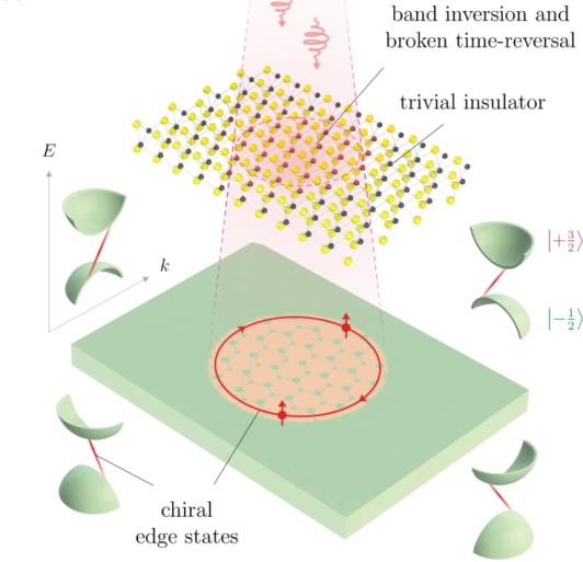
Synthesis of Lateral Heterostructures of Semiconducting Atomic Layers
Xin-Quan Zhang, Chin-Hao Lin, Yu-Wen Tseng, Kuan-Hua Huang, Yi-Hsien Lee*
citations:310
Y. Z. Hsu Scientific Paper Award (第十三屆 有庠科技論文獎)
Dielectric Screening of Excitons and Trions in Single-Layer MoS2
Y. Lin, X. Ling, L. Yu, S. Huang, Yi-Hsien Lee, J. Kong, M.S. Dresselhaus, Tomás Palacios*
citations:591
Graphene-MoS2 Hybrid Technology for Large-Scale Two-Dimensional Electronics
L. Yu, Yi-Hsien Lee, X. Ling, E. Santos, Y.C. Shin, Y. Lin, M. Dubey, E. Kaxiras, J. Kong, H. Wang, T. Palacios*
citations:661
Raman Enhancement Effect on the Two-dimensional Layered Materials:
graphene, h-BN and MoS2
X. Ling, W. Fang, Yi-Hsien Lee, P.T. Araujo, X. Zhang, J.F.R. Nieva, Y. Lin, J. Zhang, J. Kong, and M.S. Dresselhaus*
citations:459
Role of the Seeding Promoter in MoS2 Growth by Chemical Vapor Deposition
X. Ling, Yi-Hsien Lee*, Y. Lin, W. Fang, L. Yu, M.S. Dresselhaus, J. Kong*
citations:732
Electronic Transport and Device Prospects of Monolayer CVD MoS2
W. Zhu, T. Low, Yi-Hsien Lee, H. Wang, D.B. Farmer, J. Kong, F. Xia and P. Avouris*
citations:457
Trion induced negative photoconductivity in monolayer MoS2
C.H. Lui, A.J. Frenzel, D.V. Pilon, Yi-Hsien Lee, G.M. Akselrod, J. Kong, N. Gedik*
citations:264
Biexciton formation in monolayer MoS2 observed by transient absorption spectroscopy
E.J. Sie, Yi-Hsien Lee, A.J. Frenzel, J. Kong, N. Gedik*
Before NTHU
(Invited Review) Large-Area 2-D Electronics: Materials, Technology, and Devices
A. Hsu, H. Wang, Y.C. Shin, B. Mailly, X. Zhang, L. Yu, Y.M. Shi, Yi-Hsien Lee, M. Dubey, K.K. Kim, J. Kong, Tomás Palacios*
Synthesis of patched or stacked graphene and hBN flakes: A route to hybrid structure discovery
S.M. Kim, A. Hsu, Paulo T Araujo, Yi-Hsien Lee, T. Palacios, Mildred S Dresselhaus, J.C. Idrobo, K.K. Kim, Jing Kong*
citations:205
Synthesis and Transfer of Single Layer Transition Metal Disulfides on Diverse Surfaces
Yi-Hsien Lee, L. Yu, H. Wang, W. Fang, X. Ling, Y. Shi, C. Lin, M. Chang, C. Chang, M. Dresselhaus, T. Palacios, L. Li, Jing Kong*
citations:713
Van der waals epitaxy of MoS2 layers using graphene as growth templates
Y.M. Shi, W. Zhou, A.Y. Lu, W.J. Fang, Yi-Hsien Lee, A. Hsu, S.M. Kim, K.K. Kim, H.Y. Yang, L.J. Li, J.C. Idrobo, Jing Kong*
citations:1045
Integrated Circuits Based on Bilayer MoS2 Transistors
H. Wang, L. Yu, Yi-Hsien Lee, Y.M. Shi, A. Hsu, M.L. Chin, L.J. Li, M. Dubey, J. Kong, Tomás Palacios*
citations:1815
Large-scale 2D electronics based on single-layer MoS 2 grown by chemical vapor deposition
H. Wang, L. Yu, Yi-Hsien Lee, W.J. Fang, A. Hsu, P. Herring, M. Chin, M. Dubey, L.J. Li, J. Kong, Tomás Palacios*
Growth of Large-Area and Highly Crystalline MoS2 Thin Layers on Insulating Substrates
K.Liu, W. Zhang, Yi-Hsien Lee, Y. Lin, M. Chang, C. Su, C. Chang, H. Li, Y. Shi, H. Zhang, C. Lai, Lain-Jong Li*
citations:2056
Highly Efficient Electrocatalytic Hydrogen Production by MoSx Grown on Graphene‐Protected 3D Ni Foams
Y.H. Chang, C.T. Lin, T.Y. Chen, C.L. Hsu, Yi-Hsien Lee, W.J. Zhang, K.H. Wei, Lain‐Jong Li*
Synthesis of Large-Area MoS2 Atomic Layers with Chemical Vapor Deposition
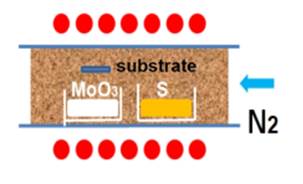
Yi-Hsien Lee, X.Q. Zhang, W Zhang, M.T. Chang, C.T. Lin, K. Chang, Y. Yu, T. Wang, C.S. Chang, L.J. Li, Tsung-Wu Lin*
citations:3543
Top ten most cited papers of Adv Mater. (461 cites in year 2017)
Electrical Probing of Submicroliter Liquid Using Graphene Strip Transistors Built on a Nanopipette
C.H. Chen, C.T. Lin, Yi-Hsien Lee, K.K. Liu, C.Y. Su, W.J. Zhang, Lain‐Jong Li*
Converting Graphene Oxide Monolayers into Boron Carbonitride Nanosheets by Substitutional Doping
T.W. Lin, C.Y. Su, X.Q. Zhang, W.J. Zhang, Yi-Hsien Lee, C.W. Chu, H.Y. Lin, M.T. Chang, F.R. Chen, Lain‐Jong Li*
Growth selectivity of hexagonal-boron nitride layers on Ni with various crystal orientations
Yi-Hsien Lee*, K.K. Liu, A.Y. Lu, C.Y. Wu, C.T. Lin, W.J. Zhang, C.Y. Su, C.L. Hsu, T.W. Lin, K.H. Wei, Y.M. Shi, Lain-Jong Li*
Opening an electrical band gap of bilayer graphene with molecular doping
W.J. Zhang, C.T. Lin, K.K. Liu, T. Tite, C.Y. Su, C.H. Chang, Yi-Hsien Lee, C.W. Chu, K.H. Wei, J.L. Kuo, Lain-Jong Li*
citations:267
Selected talk
Invited talk,
Yi-Hsien Lee, “Engineering Materials Genome of Artificial 2D Lattices“,
Stanford University, Stanford, USA, Mar. 13 (2018)
Yi-Hsien Lee, “Engineering Materials Genome of Artificial 2D Lattices“,
Stanford University, Stanford, USA, Mar. 13 (2018)
Invited talk,
Yi-Hsien Lee, "Heterostructure and Applications of monolayer semiconductors",
ISSS8, Tsukuba-Japan, Oct. 24, (2017)
Yi-Hsien Lee, "Heterostructure and Applications of monolayer semiconductors",
ISSS8, Tsukuba-Japan, Oct. 24, (2017)
Invited talk,
Yi-Hsien Lee, "Synthesis and heterostructure of monolayer semiconductors",
Recent Progress in Graphene/2D Research (RPGR), Seoul-Korea, Sep. 25, (2016)
Yi-Hsien Lee, "Synthesis and heterostructure of monolayer semiconductors",
Recent Progress in Graphene/2D Research (RPGR), Seoul-Korea, Sep. 25, (2016)
Invited talk,
Yi-Hsien Lee, "Enabling monolithic 3D image sensor using large area monolayer TMD and logic/memory hybrid 3D+IC ",
VLSI Symposia, Honolulu-US, June 16, (2016)
Yi-Hsien Lee, "Enabling monolithic 3D image sensor using large area monolayer TMD and logic/memory hybrid 3D+IC ",
VLSI Symposia, Honolulu-US, June 16, (2016)
Invited talk,
Yi-Hsien Lee, "Synthesis and Heterostructures of Monolayer Semiconductors ",
Yale University, US, Dec. 11, (2015)
Yi-Hsien Lee, "Synthesis and Heterostructures of Monolayer Semiconductors ",
Yale University, US, Dec. 11, (2015)
Invited talk,
Yi-Hsien Lee, "Heterostructures and optoelectronics of Monolayer Semiconductors ",
EE-UIUC, US, August 10, (2015)
Yi-Hsien Lee, "Heterostructures and optoelectronics of Monolayer Semiconductors ",
EE-UIUC, US, August 10, (2015)
Invited talk,
Yi-Hsien Lee, "Synthesis and Heterostructures of Monolayer Semiconductors ",
MIT-Harvard Center for Excitonics, US, August 6, (2015)
link
Yi-Hsien Lee, "Synthesis and Heterostructures of Monolayer Semiconductors ",
MIT-Harvard Center for Excitonics, US, August 6, (2015)
Invited talk,
Yi-Hsien Lee, "New Materials for Nano-photonics",
City College of New York, US, June 30, (2015)
Yi-Hsien Lee, "New Materials for Nano-photonics",
City College of New York, US, June 30, (2015)
Invited talk,
Yi-Hsien Lee, "Synthesis and Heterostructures of Two-Dimensional Atomic Layers",
APS, March Meeting, San Antonio, USA, Mar. 4, (2015)
Yi-Hsien Lee, "Synthesis and Heterostructures of Two-Dimensional Atomic Layers",
APS, March Meeting, San Antonio, USA, Mar. 4, (2015)
Invited talk,
Yi-Hsien Lee, “Synthesis, Analysis and Heterostructures of 2D Materials“,
colloquium of Physics & Astronomy, Wyoming University, US, Feb. 28 (2014)
Yi-Hsien Lee, “Synthesis, Analysis and Heterostructures of 2D Materials“,
colloquium of Physics & Astronomy, Wyoming University, US, Feb. 28 (2014)
Invited talk,
Yi-Hsien Lee, “Synthesis and Analysis of 2D Materials Beyond Graphene“,
1st Cross-Strait Workshop on Novel Quantum Materials, Taiwan, Dec. 26 (2013)
Yi-Hsien Lee, “Synthesis and Analysis of 2D Materials Beyond Graphene“,
1st Cross-Strait Workshop on Novel Quantum Materials, Taiwan, Dec. 26 (2013)
Invited talk,
Yi-Hsien Lee, “Synthesis of Transition Metal Dichalcogenides Monolayer with Aromatic Molecules“,
MRS Fall
Meeting, Boston, US, Dec. 3 (2013)
Yi-Hsien Lee, “Synthesis of Transition Metal Dichalcogenides Monolayer with Aromatic Molecules“,
MRS Fall Meeting, Boston, US, Dec. 3 (2013)
Invited talk,
Yi-Hsien Lee, “Synthesis, Transfer and Characterizations of TMD monolayers“,
Surface Science Group, Tokyo University, Tokyo, Sep. 12 (2013)
Yi-Hsien Lee, “Synthesis, Transfer and Characterizations of TMD monolayers“,
Surface Science Group, Tokyo University, Tokyo, Sep. 12 (2013)
Invited talk,
Yi-Hsien Lee, “Synthesis, Applications and Heterostructures of Two Dimensional Materials“,
Physical Sciences Seminar Series, IBM Research Center, New York, USA, Aug. 23 (2013)
Yi-Hsien Lee, “Synthesis, Applications and Heterostructures of Two Dimensional Materials“,
Physical Sciences Seminar Series, IBM Research Center, New York, USA, Aug. 23 (2013)
Invited talk,
Yi-Hsien Lee, “Synthesis and Analysis of 2D Materials Beyond Graphene“,
The 3rd Young Investigator Conference, Massachusetts Institute of Technology (MIT), USA, Aug. 1 (2013)
Yi-Hsien Lee, “Synthesis and Analysis of 2D Materials Beyond Graphene“,
The 3rd Young Investigator Conference, Massachusetts Institute of Technology (MIT), USA, Aug. 1 (2013)
Contributed talk,
Yi-Hsien Lee et al, “Synthesis of Single Layer Transition Metal Dichalcogenides with Chemical Vapor Deposition”
APS March Meeting, Baltimore, US Mar. 19, (2013)
Yi-Hsien Lee et al, “Synthesis of Single Layer Transition Metal Dichalcogenides with Chemical Vapor Deposition”
APS March Meeting, Baltimore, US Mar. 19, (2013)