Introduction
�� ��G�L����(Che-Yi Lin)
English�G������(Chih-Jie Yang)
|
�n��q���h�����t�h�᪺������
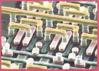
SEM image of two-level Al(Cu) interconnect lines with W-plug vias on a Si surface.
IBM J. of Res. & Develop., July 1995 |
�b�n��q��(Integrated circuit, IC)���ɽu���ƿ�ܤ��A�ѩ�ɪ��ݬ۸����L���ݦ��ۨ}�n���ɹq�ʥH�Φ������C���u�I�A�]���ɤU���n��q���s�{�j�h�O�H�ɰ������ݾɽu�����ơC�M�Ө̴`�ۼ����w��(Moore’s law)�A�������q�l����K�פ��_�W�ɡA�N�ۦb��쭱�n���n�ӤJ���q�l����ƥؤ]�j�T���W�ɡA�ӹq�����������ݾɽu�ؤo�]�j�T�Y��C�]���ɾɽu����쭱�n�ҳq�L���q�y�K�פ]�j�T�����C�b�ɾɽu���A���ɽu�������q�y�K�ר�F106 A/cm2�ɡA�]�j�q���q�l�y�����ɭ�l�y���ʶq�ಾ�A�ϱo�ɭ�l�|�̴`�۪��q�y��V�i��E���欰�A���{�H�٬��q�E��(Electromigration)�C�ӻɭ�l���q�E���|�b�쥻����m�d�U�@�ӪŤ�(Vacancy)�A�Ťժ��@�|�H�۳q�q�ɶ����W�ɦӼW�[�C�̫�ŤջE���Φ����[���լ}(Void)�A���լ}�H�۳q�q�ɶ��i�@�B�X�j�A�̲ױN�|�y���ɽu���_�u�A�Φ��u���C�]���ɭ�l���q�E���欰�P���i�a���������C
As the demand of high performance for electric component keep rising, it is necessary to scale down the integrated-circuits (IC) dimension to incorporate more semiconductor devices into a single chip. Traditional aluminum metallization has reached the limitation on fabrication of desired high speed devices. Copper metallization emerged as a promising substitution due to its low resistivity and acceptable cost. The increase in interconnect complexity together with the shrinkage of copper interconnect dimension requires finer interconnect pattern and hence increases current density passing through metal interconnect. Electromigration takes place when the current density in copper metal interconnects is over 106 A/cm2. Electromigration is the movement of the atoms in a metal line due to the momentum transfer between conducting electrons and diffusing metal atoms. Vacancies form as the atoms are bombarded away. As the momentum transfer continues, the vacancies form and coalescence into voids which might further fail the device. To increase the stability of copper interconnects, it is crucial to understand the electromigration behaviors of copper.
|
|
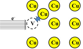
�q�E���ܷN��
Schematically illustration of electromigration. |
C. K. Hu et al., APL, 78, 904 (2001) |
�b������Ǫ���s�A�ѶW���u�Ŭ�z���q�l��L�誺�{���[���ɭ�l���q�E���欰���o�{�A�ɭ�l�����ʷ|�b�������ɳB�������C�]���Y��b�ɪ��ݤ����ޤJ�j�q���������c�A������q�E������O�]��j�T���ɡC�Ӧ��j�q�`�̤ث��������c���ɽ��b���m�W�ҩ��㦳�۷��}�n������ʽ�H�ξɹq�ʡA�b���ӻɾɽu�L���c��ܤ��O�۷��A�X����ܡC
It was found that nano-twinns can effectively increase copper mechanical strength by one order without sacrifice it electrical conductivity. By high resolution transmission electron microscopy (HRTEM), it was founded that electromigration of copper is delayed at a twin boundary in our previous research. Effective mechanical strengthening, acceptable electrical resistivity and better EM resistance makes nanotwinned copper an ideal material for advanced microelectronic applications.
|
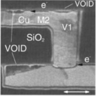
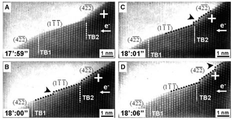
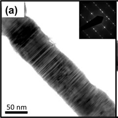
��z���q�l��L���{���[���������ɧ���ɭ�l�q�E���欰
Electromigration of copper is delayed at a twin boundary.
K. C. Chen et al., Science 2008, 321, 1066-1069
(������Ǭ�s���G/Our work) |
������ǧQ�ιq�᪺�覡�s�ƨ㦳�`���������c���ɽ��H�Ω`�̽u�C�i�ǥѹq��G���K�[���ӽձ��ɽ��������A�α��Q�q��L�{�����P������Ѽƹ���������c���K�׳y�����v�T�C���ǥѶ�����ƾT�ҪO���U�q�᪺�覡�i�s�ƥX�j�q�ӧ��ê��ɩ`�̽u���c�A�Ӧb�䤤�]���\�ޤJ�j�q���`���������c�C�㦳�j�q�`���������c���ɽ��㦳���j�ץH�Ψ}�n���ɹq�ʡA�ӥ�����ǥ�o�{�����ݪ��G�k�欰�]��W�[�����O�C
In our lab, nanotwinned copper films and nanowires are prepared by electrodeposition. It was found the growth direction of copper films can be controlled the by using proper additives. The influence of deposition parameters on twin density is another research topic. Nanotwinned copper nanowires were successfully fabricated by anodic aluminum oxide (AAO) template-assisted electrodeposition. It was also founded twinning induced grain boundary transformation can effectively delay corrosion.
 |
|
�ǥѲK�[���令����V�A���ǥ��������c�o�찪�j�ת��ɽ�
The growth direction of copper films was controlled the by additives.
T. C. Chen et al., Cryst. Growth. Des. 2011, 11, 4970-4974
(������Ǭ�s���G/Our work) |
�ҪO���U�覡�q��s�Ʃ`���������c���`�̽u
Nanotwinned copper nanowires fabricated by AAO template-assisted electrodeposition.
(������Ǭ�s���G/Our work) |
|
 |
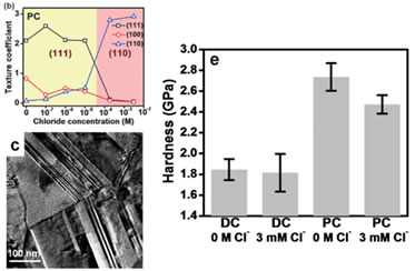
�����Φ����H���C��q���ɦ��Ī��תu���G�k
Twinning induced grain boundary transformation can effectively delay corrosion.
(������Ǭ�s���G/Our work)
|
Recent Researches (*Click on topic to read more)
Degree |
�Ӥh |
Name |
�c�h�� |
| Master |
Yi-Cang Lu |
Direction |
�Q�q��ūP�q�y�K��q��ɩ`�̽u���L���c�v�T |
| Discuss the Influence of electrodeposition temperature and current density on microstructure of
Cu nanowires. |
|
�q��ūP�q�y�K��ɩ`�̽u�L���c�v�T����s |
| Influence of electrodeposition temperature and current density on microstructure of
Cu nanowires. |
�����籴�Q�b�߽Ĺq��s�{���A�q��ūפιq�y�K��ɩ`�̽u��������V���������c�ͦ����v�T�C�ǥѼҪO���U�q��k�A�b�ӥζ�����ƾT�ҪO�����q��`�̽u�C�ñĥί߽Ĺq�᪺�覡�A�b���P�q��ūפιq�y�K�פU�s�ƻɩ`�̽u�A�A�i����Ƥ��R�C�ӥ�X������¶�g���M��z���q�l��L�誺�[��o�{�A�b���q�y�K�פU�A���C�q��G�ūצ��U�ɻɩ`�̽u�� (111) ����¶�g�j�סA�P�ɩ`�̽u�����������������Z�]�|�U���F�Ӧb�C�����Ҥ��A�����q�y�K�פ]�|���ɻɩ`�̽u�� (111) ����¶�g�j�סA�ө`�̽u�����������������Z�]�H���U���C
The objective of this study is to investigate how deposition temperature and current density affect crystal orientation and formation of twinning structure of copper nanowires in pulsed electrodeposition system. X-ray diffraction (XRD) and transmission electron microscopy (TEM) are used to analyze the crystal orientation and twin structure formation of copper nanowires, respectively. Experiment results show that the (111) crystal plane diffraction intensity of copper nanowires increases, but the average twin spacing of copper nanowires decreases with the decrease of electrolyte temperature. Moreover, with increasing current density, the (111) crystal plane diffraction intensity of copper nanowires increases, while the average twin spacing of copper nanowires decrease.
����/Hide
Degree |
�Ӥh |
Name |
���R�� |
| Master |
Li-Chien Tseng |
Direction |
�Q�q��ūP��O��q��ɽ����L���c�v�T |
| Discuss the Influence of electrodeposition temperature and current density on microstructure of
Cu nanowires. |
|
�ūP��O��߽Ĺq��s�ƻɽ��L���c�v�T����s |
| The Effects of Temperature and Substrate on Microstructure of Copper Films Prepared by Pulsed Electrodeposition. |
�]���L�q�l�n��q������ؤo���_���L�Y�A���F���ɤ��i�a�סA�A�ѹq��s�{�Ѽƹ�ɪ��ݾɽu�L���c���v�T�O�@�ӭ��n�����D�C�ɪ��L���c�P���馨�����u���V�|����q��ɪ��L�q��B�q��G�������B��O�H�ηūת��v�T�C�b����s���A�D�n�O���Q��O�P�q��G�ū�߽Ĺq��s�{�һs�ƻɪ��ݽ��L���c���v�T�C������ұĥΪ���O�A�@�����⪺����ݺ�A���ƫܱj��(200)�����u���V�A�t�@��O���Q�κϱ��q��k�b����O�W�I�n�������C�q��G���ūh����b���-1��20�סC���ۧQ���[��P����U�ɽ��������λ��B�u���V�����������Z�@�����Q�C���絲�G�o�{�A���ū��C�ɡA�Q�Ωw�q�y�Ҧ��U�i��߽Ĺq�����X���ɪ��ݽ�������������ơA�B�b�q��L�{�����骺�L�q��]���Ҵ��ɡC�����C�ūצӳy�����L�q��W�ɨϻɽ����ֳt�v�W�ɡA�i�Өϴ��ɲӤơA�ӱo��������㪺�����C�t�~�[�����q��G���ūױ���b���20�ɡA��l�q�᪺�ɽ��~�ӤF��O���u���V�A�ӷ��ūפU���ɡA��l�q�᪺�ɽ����O������������C�ɭP���t�����D�n��]�b��ūפU���ҳy�����L�q�촣�ɨϱo�U�ͪ���V���֩һݭn����q���j�T�U���A�ɭP���ɦU��V�����ֳt�רS������t���ӱo��L�S�w�u���V�������C�̫�]�[�����ū��C�ɡA�������c�����Z�j�T���U���C�����ūפU����A�ɽ��������O�]�b�C�Źq��U���ּƶq���h�δ��ɸ��h�Ӧ��Ҵ��ɡA�t�~�b�C�ŤU�A�������O����N�Ѯt�ƷƲ����ܦ��Φ��`������������A�ϧC�ŤU�s�ƪ��ɽ������������c�o�K�CElectrochemical deposition is commonly employed in the fabrication of copper interconnects owing to its low cost advantage and ease of mass production. To further down scaling the microelectronic device, more in-deep knowledge and process control concerning interconnect microstructure are required to improve device reliability. Copper film microstructure is known to be tailored by various process parameters such as electrodeposition overpotential, electrolyte composition, substrate and temperature. In this study, nanocrystalline copper films were fabricated by galvanostatic pulsed electrodeposition using an addictive-free sulfate solution as an electrolyte. In comparison, two types of substrate have been used: one is a commercial nickel foil with strong (200) texture and the other is copper film prepared by sputtering which has no preferred orientation. The electroplated copper films were deposited at -1 and 20�aC. The surface topology, morphology, crystallographic texture and twin spacing distribution of the copper films electrodeposited under various conditions were examined. In this experiment, we observed that as the deposition temperature decreases, the copper film showed an increase in the deposition overpotential and a decrease in surface roughness. The inheritance of substrate texture in the electrodeposited copper film was found to be tailored by deposition temperature. As the deposition temperature decreases, the deposits show less dependent on the crystallographic orientation of the substrate. It was also found that twin spacing lamella reduces with decreasing deposition temperature. We proposed that the increase of overpotential has significant influence on the nucleation behavior. The increase of overpotential leads to higher nucleation rate and lower growth rate of existing nuclei, thus a smoother surface was obtained. At lower deposition temperature, the probabilities of nucleus formation on varies planes are generally the same, thus the electrodeposited copper films did not show any preferred orientation. Finally, the decrease of twin spacing was believed to be associated with the increasing stress caused by high nucleation rate under low deposition temperature.
����/Hide
Degree |
�Ӥh |
Name |
������ |
| Master |
Chih-Jie Yang |
Direction |
�Q�q��ɽ������������c��Benzotriazole(BTA)��ܻG�k��O���v�T |
| Discuss the Influence twin structures and BTA on the corrosion properties of electrodeposited copper films. |
|
�`�������q����������G�k�S�ʬ�s |
| Corrosion Properties of Nanotwinned Copper Films Prepared by Electrodeposition.
|
�b�n��q���ɳs���ɽu�s�{���A�ƾǾ����i�O�����L�h���ƥH�ξ㥭�դ������̭��n����k�C�Ӧb�ƾǾ����i���ĥΪ��߮ƫo���s�{�a�ӤF���G�k�����T�w�]���C�ƾǻG�k�H�Φ��˥��G�k���`�y������}�v�L�C�άO���C��i�a�סA�]�������ɧܻG�k��O�����������n��ij�D�C
��~�ө`�������ɦ]�㦳������j�צP�ɫO���}�n���q�ɲv�Χܹq�E������O�ӳQ�s�x��s�A����ܻG�k��O�o�q�����H���Q�C�]������s�ǯ߽Ĺq��s�{�I�n���������c���ɽ��A�ì�s�������c�O�_�ണ�ɧ��ƧܻG�k��O�CBenzotriazole (BTA)�Q�s�x���Φb�ƾǾ����i���@���ܻG�k���A�P�ɥ禳���Φb�q�ᤤ�@���K�[���H�Ӥƴ��ɡA�Ϫ�������C���o�u�����֤��m���@���K�[���O�_��P�ɴ��ɹq��ɽ����ܻG�k��O�Q�סC�]������s����w��HBTA�@���K�[�����q��ɽ��ܻG�k��O���Q�סC
In copper interconnects of integrated circuit process technology, chemical mechanical polish (CMP) is the most important step to remove overburden material and planarize surface of metallization. However, the slurry adopted in CMP may introduce corrosion issue. Chemical and galvanic corrosions of copper interconnects during processing may cause the failure of device. Therefore, it is crucial to find a way to increase the corrosion resistance of copper interconnects.
Nanotwinned copper has received broad attention recently due to its high mechanical strength, reasonably low electrical resistivity, and better electromigration resistance. However, its corrosion resistance is yet to be investigated. In this research, the corrosion resistance of nanotwinned copper prepared by pulsed electrodeposition technique is studied. Benzotriazole (BTA) is widely applied as a corrosion inhibitor in CMP and an electrodeposition additive as a brightener. But there is only limited literatures addressing the corrosion resistance of copper films deposited with BTA. In this study, the corrosion resistance of copper films electrodeposited with BTA is investigated.
����/Hide
Degree |
�Ӥh |
Name |
�L���� |
| Master |
Che-Yi Lin |
Direction |
��s�b�C�����ҤU�A���P�q�y�Ҧ��q��s�ƻɽ���������V�H�Ϊ����λ��A�H�Ω`���������c�H�ū��ܤƪ��i�����C |
| Discuss the influence of different current modes on the growth direction, surface roughness and nano-twin structures. |
|
�C�����ҤU�q��ɽ����ʽ��s |
| Characterization of Cu films prepared by electrodeposition at low temperature. |
�b�q�l���s�{���A���ݾɽu����J�D�n�O�Q�ιq�᪺�覡�C���F�DzΪ����y�q��~�A�߽Ĺq��]�Q�s�x�����Φb���P���s�ƻݨD�W�C�M�Ӧb�q�᪺��s���A����q��G�ūת����Q����ʥF�A�ר�b�ǷťH�U�q��s�{����s�D�`�}�֡C���~�A�㦳�`���������ɪ��ݦ]�㦳������j�ץH�Ψ}�n���ɹq�ʡA�b��~�ӳQ�s�x����s�A�Ө䤤�@�ػs�Ƥ覡�N�O�ĥί߽Ĺq��A�ӻɽ������������Z�P�߽Ĺq�y���q�y�K�ץH�Φ��Įɶ������A�����ūת��v�T�èS����������s�C�G�b����s���N���Q���y�q��H�ί߽Ĺq��b���P�ūפU���v�T�A�ñ��Q�ū������q��Φ��������v�T�C
Electrodeposition is the most commonly used method for depositing Cu metallization in microelectronic devices. Both direct-current and pulsed current application modes have been used in the electrodeposition process. Although electrodepostion temperature is a critical parameter to control the properties of deposited metal, very few research efforts have been dedicated to investigate the electrodeposition process at low temperature regime. Recently, Cu with high-density nanoscale twins has received extensive attention due to its high mechanical properties and decent electrical conductivity. In previous works, Cu with nanoscale twins could be fabricated by pulsed electrodeposition. Twin thickness was found to be related to the current density and duty cycle during the pulsed electrodeposition process. However, the influence of temperature has not been investigated yet. In this study, the effects of deposition temperature and deposition current mode on the microstructure of the electrodeposited Cu films are the subjects of interests.
����/Hide�@
��s����G
2012-08-07