-
 Congratulations to membersContinue Reading »
Nov. 17, 2021
Prof. Yi-Hsien Lee (李奕賢老師)
獲選 2021 全球高引用學者 (連續三年)
Nov. 19, 2020
Prof. Yi-Hsien Lee (李奕賢老師)
獲選 2020 全球高引用學者
Dec. 12, 2019
Dr. Ying-Yu Lai (賴映佑, Postdoc)
獲得 2020 愛因斯坦學者 研究經費
Nov. 13, 2019
Prof. Yi-Hsien Lee (李奕賢老師)
獲選 2019 全球高引用學者
Nov. 13, 2019
Dr. Tung-Han Yang (楊東翰, Postdoc)
獲得 2020 愛因斯坦學者 研究經費
Aug. 13, 2019
Dr. Ying-Yu Chen (賴映佑, Postdoc)
MoST funding for oversea research in U. Michigan (Phys.)
Aug. 05, 2019
P. Y. Chen (陳柏諺, PhD)
Cover of Adv. Mater.
Jul. 20, 2019
P. Y. Chen (陳柏諺, PhD)
Online publication of Adv. Mater.
Nov. 28, 2018
Dr. Tung-Han Yang (楊東翰, Postdoc)
獲得 科技部 千里馬博士後獎學金(Stanford University - MSE)
Nov. 20, 2018
ANGEL Lab (李奕賢 教授實驗室)
獲選 清華大學 全校十大重點研究
Feb. 15, 2018
K.C. Chiu (邱冠璋, PhD)
Cover of Adv. Mater.
Feb. 14, 2018
Tung-Han Yang (楊東翰, PhD)
Back cover of Adv. Func. Mater.
Jan. 1, 2018
Prof. Yi-Hsien Lee (李奕賢老師)
獲選 自然司-奈米科技創新應用學門
複審委員
Dec. 13, 2017
Tung-Han Yang (楊東翰, PhD)
Jerry, P.H. Chen (陳柏翰, PhD)
Paper published on Nano Letters
Oct., 2017
Meng-Hsi Chuang (莊孟熹, PhD)
Paper published on Nano Letters
Aug., 2017
Cheng-Tse Chou, (周成澤, Master)
Wei-Chun Ko (柯維俊, Master)
Paper published on Nano Letters
Nov. 2, 2016
J.A. Chen (陳俊安, PhD)
Jerry, P.H. Chen (陳柏翰, PhD)
Scholarship of the best PhD Rookie,
NTHU President Award, 2016
清華大學博生 校長四年獎學金
Oct.5. 2016
Y.C. Chiang (undergrad, 系排1/121)
Scholarship of the best MSE talent, Academia Award, 2016
第二屆清華材料”領袖材子”
菁英獎學金 15萬
K.W. Tseng (undergrad, 系排10/121)
第二屆清華材料”領袖材子”
菁英獎學金 5萬
C.C. Lee (undergrad, 系排2/121)
俞國華獎學金 5萬元
Sep. 28, 2016
Prof. Yi-Hsien Lee (李奕賢老師)
3-year research award of US Navy & US Airforce
Grant No. FA2386-16-1-4009
Aug. 1, 2016
Prof. Yi-Hsien Lee (李奕賢老師)
MOST 3-year funding
自然司物理學門: 105-2112-M-007 -032 -MY3
自然司尖端晶體: 105-2119-M-007 -027
May 2, 2016
P.H.Chen (陳柏翰, PhD)
Scholarship for half-year exchange program
@UIUC-EECS(清華大學學海計劃)
Apr. 29, 2016
曾郁雯 (碩一)
工學院論文競賽
口頭組 材料系第一名
黃冠華 (碩一)
工學院論文競賽
海報組 材料系第一名
Mar. 16, 2016
K.C. Chiu (邱冠璋, Ph.D.)
M.H. Chung (莊孟熹, Ph.D)
C.T. Chou (周成澤, master)
C.N. Laio (廖昶寧, master)
paper accepted - VLSI
Mar. 10
大三專題生 蔣宜成 (系排1/120)
朱順一獎學金 十萬元
Dec. 1, 2015
K. C. Chiu (邱冠璋, Ph.D.)
Scholarship for one-year exchange program
@IBM-TJ Watson Research Center
(科技部千里馬 scholarship)
November, 2015
大四專題生
陳俊安(系排1/125)
陳柏翰(系排6/125)
清華材料 大學生菁英逕博獎學金
Nov. 12, 2015
JA Chen (陳俊安, 材料大四)
PH Chen (陳柏翰, 材料大四)
PZ Wang (王培儒, 動機大四)
3 undergrad. talents get permission for
Ph.D. program in ANGEL lab
Jul. 02, 2015
Prof. Yi-Hsien Lee (李奕賢老師)
榮陞 副教授
Jun. 08, 2015
J. A. Chen (陳俊安, undergrad.)
Scholarship of the best MSE talent, Academia Award, 2015
第一屆清華材料”領袖材子”
研究菁英獎學金20萬元
May 18, 2015
Prof. Yi-Hsien Lee (李奕賢老師)
New Faculty Research Award, National Tsing Hua University, 2015
第五屆 清華工學院新進人員研究獎
May 08, 2015
Prof. Yi-Hsien Lee (李奕賢老師)
Y. Z. Hsu Scientific Paper Award 2015
第十三屆 有庠科技論文獎
May 1, 2015
Prof. Yi-Hsien Lee (李奕賢老師)
Highlighted with the news of “Science”
“BEYOND GRAPHENE”,
Science, 348, p.490-492 (2015)
專訪內容 刊登於”科學”專欄新聞
Apr. 15, 2015
Y. W. Harn (韓羽唯, master)
Admissions & scholarship for PhD program
@ UC Berkeley
@ Georgia Tech.
April 1, 2015
M. S. Chuang (莊孟熹, Ph.D.)
Scholarship for half-year exchange program
@ EECS - UIUC
(優等生學逕博 scholarship)
Mar. 12, 2015
Funding support for oversea research
@IBM-TJ Watson Research Center"
(清華大學蹲點計畫)
Feb. 1, 2015
Xiaoze Liu (劉曉澤, 紐約城市大學物理博士)
科技部新增補助 "清華大學延攬客座科技人才"
(MOST 104-2811-M-007-007)
Jan.uary 15, 2015
E. C. Lin (林爾震, undergrad.)
paper published on Nature Photonics
Dec. 11, 2014
X. Q. Zhang (張鋅權, Ph.D.)
C. H. Lin (林璟豪, Master)
Y. W. Tzeng (曾郁雯, undergrad.)
K. H. Huang (黃冠華, undergrad.)
paper published on Nano Letters
Dec., 2014
T. H. Yang (楊東翰, Ph.D.)
Scholarship for two-year-oversea-research program
Younan Xia's Group @ Georgia Tech
(千里馬 scholarship)
Nov., 2014
大四專題生林爾震
清華材料 學逕博正取
Nov., 2014
大四專題生曾郁雯、黃冠華、周成澤
清華材料碩甄, 全數正取
Oct. 30, 2014
大四專題生曾郁雯、黃冠華、周成澤
清華工科碩甄, 全數逕行錄取
-
 One-molecule-thick material has big advantagesContinue Reading »
The discovery of graphene, a material just one atom thick and possessing exceptional strength and other novel properties, started an avalanche of research around its use for everything from electronics to optics to structural materials. But new research suggests that was just the beginning: A whole family of two-dimensional materials may open up even broader possibilities for applications that could change many aspects of modern life.
-
 New wonder material to rival graphene?Continue Reading »
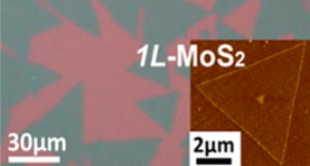
A team from MIT believes molybdenum disulphide (MoS2) could enable new electronic materials and devices, including clothing with embedded electronics and glasses with built in displays.
While molybdenum disulphide has been used in industry for many years as a lubricant, it wasn't considered to have application in electronic devices. However, scientists at the Swiss university EPFL produced a transistor on the material last year and the MIT researchers now believe it has the potential to rival graphene.
-
 Lab website has launched We are pleased to announce the ANGEL Lab has launched a new website.
What is 2D material?
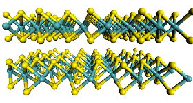
Recently, there has been enormous progress in the production of atomic crystals that are strictly two dimensional (2D) and can be viewed as individual planes of atomic-scale thickness pulled out of bulk crystals like graphite, h-BN, several transition metal dichalcogenides (TMD), and complex oxides. By stacking various atomic crystals on top of each other, it is possible to create multilayer heterostructures which hold the promise for novel devices with designed electronic properties. For instance, concepts for novel transistors based on lateral and vertical transport as well as optoelectronics have been proven.
While obviously promising for applications, these new materials are very different from usual three dimensional bulk materials, as now all atoms are very close to a surface or some interface and vertical quantum confinement or stacking control properties like electronic gaps. Reduced dimensionality is generally expected to affect heat and charge transport in these novel materials. However, a coherent understanding of how to control the electronic properties of new 2D materials and, particularly, a unifying “standard model” of these novel hybrid materials, remains to be built.
Research on low dimensional materials is driven both by fundamental scientific questions and the perspective of applications. For instance, electrons in graphene – an atomically think sheet of carbon – behave like massless Dirac particles and exhibit remarkably high mobilities even though graphene is an all surface material and electrons are directly exposed to perturbations from its environment. These properties are prospective for applications like, e.g., ultra-high frequency transistors and novel “vertical” electron tunnelling transistors. Similarly, a single layer MoS2 proved very promising for transistor applications.
Continue Reading »