Photocatalysis and Smart Sensor Materials
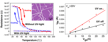
We have discovered the VO2 microwires’ photo-induced phase transition mechanism using an ultraviolet-light. On the obtained VO2 nanowires, the photo-induced insulator-to-metal (IM) phase transition occurred from monoclinic (insulator or semiconductor) to tetragonal (metal) structures at room temperature. The photocurrent to dark current ratio of the nanodevice was at 285 fold with ultra-short response and recovery times of 1.3 and 4.5 milliseconds (ms), respectively, at 7µWcm-2 of UV-light intensity. As UV-light intensity increased to 2.33mWcm-2, a maximum photocurrent to dark current ratio of 719 fold was observed. A high-resolution transmission electron microscopy (HRTEM) image indicates that the nanowires grew along the [100] axis as a single crystal. The VO2 nanowires were then fabricated into field-effect transistor (FET) devices. High electron mobility of 29 and 7.93 cm2V-1S-1 were obtained with UV on (2.33mWcm-2) and off, respectively. The electrical properties of photo-induced IM phase transitions of VO2 nanowires were investigated. were investigated.
Photocatalysis and Ultraviolet-light assisted thermal decomposition process ZnO Nanostructures.
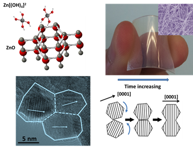
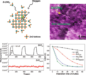
In ambient air, zinc acetylacetonate hydrate precursor was directly decomposed to fabricate large-area ZnO nanowires on substrate using ultraviolet-light (λ=350-380nm, I=76 mWcm-2) assisted thermal decomposition processes at 200oC. The growing process required 5 minutes. High-resolution transmission electron microscopy images revealed that the ZnO nanowires consist of fine single-crystal nanoparticles. The particle size is ~8-9 nm using Debye-Scherrer equation for evaluation. The photocatalytic activities of ZnOnonUV (without UV-light assistance) nanowires were superior to those of ZnOUV (with UV-light assistance) nanowires and commercial TiO2 P25 nanoparticles. The oxygen defects (i.e., oxygen vacancies and interstitials) acted as key components for a high photodegradation process in ZnO nanowires. The oxygen defects are attributed to the presence of Zn(OH)2 on the surface of ZnO nanocrystallines. For the photoresponsive activities, no significant photocurrent to dark current ratio was observed in ZnOnonUV nanowires, using UV-light (λ=365nm, I=2.33 mWcm-2) while that of ZnOUV nanowires was high, reaching a maximum of 91 fold. As-synthesized ZnOUV nanowires exhibited a relatively good crystallinity and superior photoresponsive properties when compared with ZnOnonUV nanowires based on the characterizations of the materials and sensor properties. Detailed mechanisms of photoresponsive and photocatalytic properties were investigated.
Rapidly Synthesized ZnO Nanowires by Ultraviolet Decomposition Process in Ambient Air for Flexible Photodetector
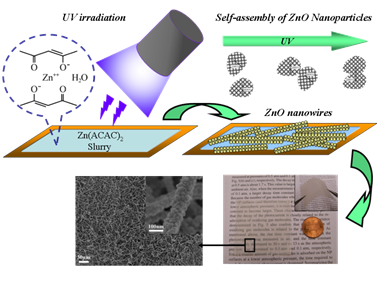
This work, a simple direct ultraviolet light was used to decompose zinc acetylacetonate hydrate precursor to fabricate ZnO nanowires on flexible substrate ambient air. ZnO nanocrystal (or nanowire) production only requires three to ten minutes. A field emission scan electron microscopy (FESEM) image reveals the high aspect ratio of the ZnO nanowires, which are grown on a substrate with a diameter of ~50-100 nm and a length of up to several hundred microns. High resolution transmission electron microscopy (HRTEM) images reveal that the nanowires consist of many single crystalline ZnO nanoparticles that grow along the c axis, which suggests an oriented attachment process. A potential application for flexible UV photodetectors was investigated using a UV lamp (λ=365 nm, I=2.34 mWcm-2). A significant ratio of photocurrent to dark current --around 11300%-- was achieved.
Room temperature photo-induced phase transitions of VO2 nanodevices
We have successfully fabricated the VO2 nanodevices using a photo-induced phase transition mechanism under an ultraviolet-light (λ=365 nm, I=7µWcm-2). On the obtained VO2 nanowires, the photo-induced insulator-to-metal (IM) phase transition occurred from monoclinic (insulator or semiconductor) to tetragonal (metal) structures at room temperature. The photocurrent to dark current ratio of the nanodevice was at 285 fold with ultra-short response and recovery times of 1.3 and 4.5 milliseconds (ms), respectively, at 7µWcm-2 of UV-light intensity. As UV-light intensity increased to 2.33mWcm-2, a maximum photocurrent to dark current ratio of 719 fold was observed. A high-resolution transmission electron microscopy (HRTEM) image indicates that the nanowires grew along the [100] axis as a single crystal. The VO2 nanowires were then fabricated into field-effect transistor (FET) devices. High electron mobility of 29 and 7.93 cm2V-1S-1 were obtained with UV on (2.33mWcm-2) and off, respectively. The electrical properties of photo-induced IM phase transitions of VO2 nanowires were investigated. were investigated.